Difference between revisions of "MEK6800"
| Line 2: | Line 2: | ||
[[File:RIMG2951b.JPG|thumb|]] | [[File:RIMG2951b.JPG|thumb|]] | ||
| − | == | + | == Specification == |
| − | + | Motorola MEK68000D2 Evaluation Kit | |
| + | * microcomputer module 84DW6232X01 | ||
| + | ** No RAM except for the jbug scratch at A000-A07f; U14,U16,U18,U19 are empty, modified to have RAM from 0000 via exorciser bus. | ||
| + | ** No extra EPROM; U10,U12 are empty | ||
| + | ** Some extra circuits: 2 6850's and a clock, perhaps an RS232 interface. | ||
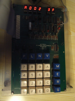
| + | * keyboard/display module 84DW6233X01 | ||
| + | * EXORciser backplane | ||
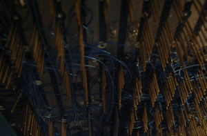
| + | * Memory module (wire-wrapped): 16 x 4116 (32KB) | ||
| − | + | == Condition == | |
| − | + | Working condition, the monitor program is usable. | |
| − | + | But the memory module doesn't work, so the only RAM is the JBUG scratch, 128 bytes at A000-A07F. | |
| − | + | Three wires are loose of the added components on the processor module. I don't know where they should go. | |
| − | I | + | I'm using a PC ATX power supply to provide 5V. |
== Data Transfer == | == Data Transfer == | ||
| Line 24: | Line 31: | ||
Now you have a binary file but it still has some headers and framing. If you strip those you have the actual ROM and it looks exactly the same as the one on [http://www.bitsavers.org/pdf/motorola/jbug.hex bitsavers] | Now you have a binary file but it still has some headers and framing. If you strip those you have the actual ROM and it looks exactly the same as the one on [http://www.bitsavers.org/pdf/motorola/jbug.hex bitsavers] | ||
| + | |||
| + | The other direction I haven't tried yet, but it's not very useful unless there is more RAM. | ||
== Done == | == Done == | ||
Reseated all chips on the memory board. No change. | Reseated all chips on the memory board. No change. | ||
Revision as of 17:43, 14 November 2010
Contents
Specification
Motorola MEK68000D2 Evaluation Kit
- microcomputer module 84DW6232X01
- No RAM except for the jbug scratch at A000-A07f; U14,U16,U18,U19 are empty, modified to have RAM from 0000 via exorciser bus.
- No extra EPROM; U10,U12 are empty
- Some extra circuits: 2 6850's and a clock, perhaps an RS232 interface.
- keyboard/display module 84DW6233X01
- EXORciser backplane
- Memory module (wire-wrapped): 16 x 4116 (32KB)
Condition
Working condition, the monitor program is usable.
But the memory module doesn't work, so the only RAM is the JBUG scratch, 128 bytes at A000-A07F.
Three wires are loose of the added components on the processor module. I don't know where they should go.
I'm using a PC ATX power supply to provide 5V.
Data Transfer
I have successfully dumped the JBUG ROM using the cassette out. Type this to Punch addresses E000-E3FF:
A002M E0G 00G E3G FFE P
Just before the P, start recording a wav file. Then process the wav using this perl script
Now you have a binary file but it still has some headers and framing. If you strip those you have the actual ROM and it looks exactly the same as the one on bitsavers
The other direction I haven't tried yet, but it's not very useful unless there is more RAM.
Done
Reseated all chips on the memory board. No change.

