Difference between revisions of "MEK6800"
| Line 21: | Line 21: | ||
A002M E0G 00G E3G FFE P | A002M E0G 00G E3G FFE P | ||
| + | Just before the P, start recording a wav file. Then process the wav using [http://www.cse.dmu.ac.uk/~mward/martin/software/index.html#CUTS this perl script] | ||
| + | |||
| + | Now you have a binary file with some headers and framing. If you strip those you have the actual rom and it looks exactly the same as the one on [ bitsavers | ||
== Done == | == Done == | ||
Reseated all chips on the memory board. No change. | Reseated all chips on the memory board. No change. | ||
Revision as of 03:04, 14 November 2010
Condition
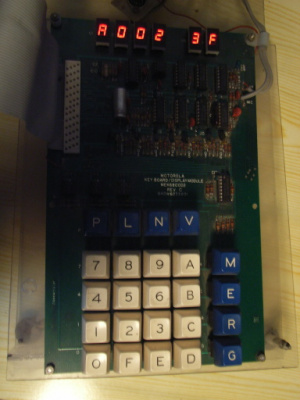
Consists of the base kit (processor board + keyboard/display board). An additional (hand wire wrapped) memory expansion board connected through an EXORciser backplane to the processor board.
Generally seems to work, the monitor program is usable.
There seems to be no RAM at the normal addresses (0000 - 00ff). Trying to change memory doesn't work there. Perhaps it is mapped elsewhere. The JBUG scratch RAM at a000 - a07f is working.
Since I don't find any RAM, I was unable to actually enter and run a program.
Some chips were added on the free space of the processor board, but three wires are loose. I don't know where they should go and it requires soldering on the processor board.
I tested using a PC ATX power supply to provide 5V to the EXORciser backplane.
Data Transfer
I have successfully dumped the JBUG ROM using the cassette out. Type this to Punch addresses E000-E3FF:
A002M E0G 00G E3G FFE P
Just before the P, start recording a wav file. Then process the wav using this perl script
Now you have a binary file with some headers and framing. If you strip those you have the actual rom and it looks exactly the same as the one on [ bitsavers
Done
Reseated all chips on the memory board. No change.

